
Exposure
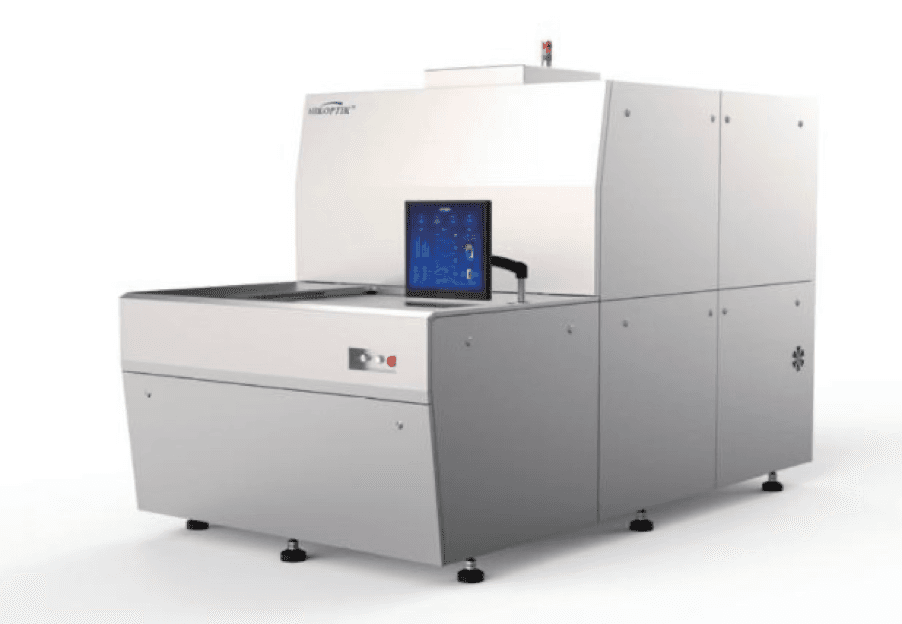
Adtech Exposure System
Adtech Exposure System is a high-precision PCB exposure solution supporting LDI, contact exposure, and direct exposure processes for HDI PCB and IC package substrate manufacturing.
Specifications
- Manufacturer
- Adtech
- Model
- INPREX / ADEX / DE
- Working Area
- PCB Panel Support
- Spindle
- -
- Speed
- High-speed one-time scan
- Power
- Laser Diode / UV Exposure
- Voltage
- Factory Spec
- Application
- HDI PCB, IC Substrate, Fine Line PCB, MLB PCB
Detailed Description
Overview
Adtech Exposure System is a high-precision exposure solution used to form circuit patterns in PCB and IC substrate manufacturing processes.
The product lineup includes INPREX, ADEX, and DE series, supporting various production requirements such as laser direct imaging, contact exposure, and direct exposure.
LDI technology enables maskless circuit pattern exposure and is suitable for high-resolution pattern formation in HDI PCB, IC package substrate, and fine line PCB production lines.
Key Features
- Supports Laser Direct Imaging (LDI)
- Available for contact exposure and direct exposure processes
- Maskless circuit pattern exposure
- High-resolution fine line pattern formation
- Auto focus function support
- Supports large-size and thick PCB panels
- Can be integrated with automatic transport systems
Applications
This system can be used for HDI PCB, IC package substrate, fine line PCB, multilayer PCB, semiconductor package substrate, and high-precision circuit board manufacturing processes.